Free Project Circuit Schematic Articles Search

Custom Search
WELCOME to "FREE PROJECT CIRCUIT SCHEMATIC"

Sponsor Links

AmericasBest.com
Showing posts with label Controller. Show all posts

Wednesday, January 16, 2013

Rolling Shutter Motor Control Circuit


This is a circuit for an electrically operated rolling shutter usually has a standard control panel with a three-position switch: up, down and stop. If you would like to automate the opening and closing with a time controlled switch, a few additional wires will have to be connected. Typically, the controls are implemented as indicated in the schematic ‘Normal Situation’. This is the figure of the circuit;


If this is indeed the case, then you can see in ‘New Situation’ how the shutter can be automated with a timer. There is only one method to determine the actual schematic of your control circuit, and that is to open the control box and using an ohmmeter, pencil and paper to check out and draw the circuit. Make sure you turn the power off first though! Connect a 230-V relay (with both the contacts and the coil rated 230 VAC) to the timer. The changeover switch between automatic and manual control needs to be rated 230 VAC as well and may not be a hazard for the user. The relay and switch are preferably fitted in a plastic mains adapter enclosure with built-in plug, which is plugged into the timer. It is a good idea to check first if this will actually fit. Because of the manual/automatic-switch, the operation is completely fail-safe and misunderstandings are out of the question. The switch prevents the issue of conflicting commands (with disastrous consequences) when, for example, the shutter is being automatically raised and manually lowered at the same time.

Sunday, January 13, 2013

GFI Ground Fault Interrupter Circuit


I always wondered what was inside one of these clever devices, so I found one in my junk box and popped the lid—it was from a defunct blow hair dryer—never throw one of these away because the GFI unit long outlives the hair dryer and has many experimental uses. To get it apart, I had to make a special screw driver bit to remove the tamper resistant screws. Here’s the figure of the design circuit;


You will notice that the parallel power leads make a single turn through the primary of the current transformer (CT). The flux field of the source lead is cancelled by the flux field in the return lead so the net result is zero and the CT sees no primary current. Should these currents ever become unequal (as in a ground fault condition), the CT senses this difference and induces current into the 1000 turn secondary. The secondary current is low, but the load resistance is 1M, so it develops significant voltage. This voltage is sufficient to exceed the comparator threshold voltage of the IC and fire the SCR. When the SCR fires, it energizes the solenoid coil and jerks an iron slug toward the center of the coil. Attached to this iron slug is a stainless steel pin that actuates the mechanical release for the electrical contacts. When the contacts are open, the ground fault current is interrupted and the appliance is off-line. It remains off until the mechanical reset button is pressed.

Friday, October 07, 2011

Downed Model Locator Circuit

Here’s a design circuit that available for your local Radio Shack store, and modified it to decrease false triggering from low voltage spikes in the on-board power system when full sized or higher torque servos are used. This circuit is called downed model locator. Your transmitter sends a set of pulses to your receiver every 20 milliseconds, and your receiver in turn sends an individual pulse to each of your servos at the same interval. This circuit is a pulse omission detector--an alarm sounds when the pulses, originating from your transmitter, are no longer present. By plugging this circuit into an unused servo socket on your receiver, you can turn on the alarm by turning off your transmitter. This figure is show about the circuit;


The first capacitor C1 filters out DC voltage, preventing an aggressive automatic gain control of some current receivers from shutting off the alarm even when your transmitter is off. The first transistor Q1 serves to flip the pulse to negative modulation that the 555 needs. The C2 capacitor and the R4 resistor establish the time interval--if no pulse is received in the time it takes to charge the capacitor through the resistor, the alarm sounds. The interval is the resistance multiplied by the capacitance: 1uF x 47k = 0.000001F x 47000 ohms = 0.047sec = 47msec which is a little over twice the standard 20msec R/C frame rate--this device uses a little longer interval than the frame rate to prevent false triggering. The other capacitor C3 smoothes the control voltage on the 555, preventing false triggering from spikes in the supply voltage. Unless a pulse opens the Q2 transistor to drain the C2 capacitor before the capacitor is fully charged, the pin 6 threshold senses a high voltage and triggers the output pin 3 to go low, sinking current across the buzzer and making noise. With the reset pin 4 high, the discharge pin 7 drains the capacitor, and the cycle starts again.

Saturday, January 29, 2011

Mixer or Sewing Machine Motor Speed Control Circuit

This circuit will be effective to use simple half wave motor speed control with small universal ac/dc motors. Two amps RMS is the maximum current capability. The control gives excellent torque characteristics to the motor because speed dependent feedback is provided, even at low rotation speeds. Here’s the figure of the circuit;


By closing switch S1, thus bypassing the SCR, we can achieve normal operation at maximum speed. [Circuit diagram source:  seekic.com]

Saturday, October 16, 2010

Motion (Motor) Control Servo System Block Diagram


This is a figure for a block diagram of a modern automated systems incorporate closed-loop feedback for motion control. They typically include a servo system that consist of feedback elements and motor driver combined in a manner. This will give accurate and stable control over speed and position. Below is the illustration of the various system-level components of a typical servo system. This is the figure of the diagram;


For processing the high-speed encoder signals, typical motion-controller cards and modules include a motion-control IC, a microprocessor, and a DSP or custom ASIC. Velocity and direction of rotation signals to the driver or amplifier is provided by the controller which in turn provides the proper levels of voltage and current (power) to operate the motor. We must have address the following items at the system level to design robust and fault-tolerant motion-control system with feedback during design: Controller-encoder input circuits (receiver circuits), Receiver circuit PC-board layout  and Encoder-signal cabling system. Motion-controller inputs, such as hard-wired emergency stop and limit inputs, should also be considered when designing a fault-tolerant feedback system though not addressed in this article.

Friday, September 17, 2010

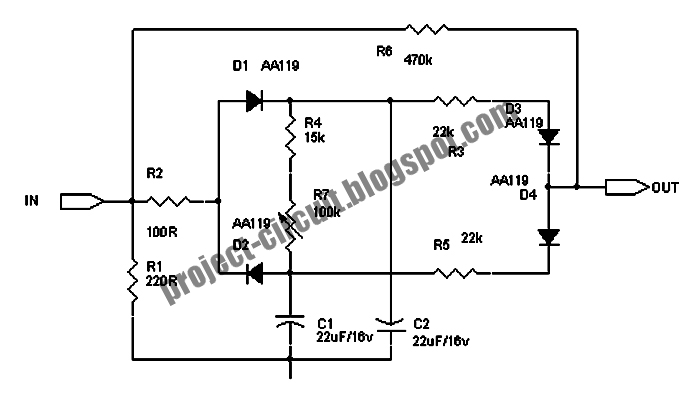
Dynamic Compressor, Self Powered Circuit


This is a circuit for dynamic compressor will give about 20dB compression, at very wide input signal range 100 mV to 10 V.  Another advantage of this circuit is that this circuit doesn’t need any power supply, we call it self powered, or more accurately, signal-powered compressor. This is the figure of the circuit;


A part of the signal is rectified by D1 and D2 and is used to charge C1 and C2 Capacitors. This current control the attenuator diodes D3 and D4, together with R3, R5, and R6.  The attenuator diodes work at the nonlinear region of the forward current curve. At low level, the input signal is not attenuated since the rectified voltage is under voltage bias of  D3 and D4, since that D3 and D4 become non-conductive.  If the level of input signal increase, at some point, the D3 and D4 begin to conduct and attenuate the signal.

The attack time of this compressor circuit is fixed and is determined by time constant of C1, C2, R2, and the output impedance of the input source that feed this compressor input. The decay time can be slightly adjusted by R7 variable resistor.  You can see that the signal  path of this compressor circuit use a 470k resistor as the attenuator, means that you should only connect the output of this circuit to a high impedance stage. This circuit works best with germanium diodes, since it has lower forward bias voltage and also smoother curve than silicon diodes.  Using silicon diodes will works but the performance would be degraded.

555 IC PWM Controller: Grounded and Ungrounded Load


This is a circuit for PWM controller circuit. While keeping the oscillator frequency relatively stable, this 555 based PWM controller features almost 0% to 100% pulse width regulation using the 100k variable resistor. To give a frequency range from about 170Hz to 200Hz , the frequency is dependent on the 100k pot and 100n. This is the figure of the circuit;


You can see the charging and discharging of the 100n cap is done through output pin 3, and this provide a push-pull symmetric drive for easy pulse-width setting. You can see two versions, the left side for grounded load, and the right side for ungrounded load. The grounded one use pin 7 to drive the transistor, while the ungrounded one use the same push-pull output pin3, this difference is needed because wen need an inverted phase to provide consistent potentiometer scale on both version.

Tuesday, August 17, 2010

Fan Control Circuit Using NTC and TL082


This is a circuit for fan control that is a simple circuit. This is the figure of the circuit;


R1 15k ohm resistor. NTC Thermistor- 10k ohm, sold at Radio Shack in the states. P1 10k ohm potentiometer - sets the low speed(voltage) of the fans at the cool temperature. P2 50K ohm potentiometer - sets the gain of the circuit - how fast the voltage will rise to full output when the temp is higher. TL082 a op-amp that I had handy, most any single voltage op-amp should work. The TL082 is a dual op-amp if you want more then one controller on a board. note that the power and ground connections for the op-amp are not shown on the schematic. R2 - The TL082 is a fast op-amp, needed R2 to reduce oscillation. IRF-510 A 4 amp mos-fet in a TO-220 case. Bascially as the voltage on the gate rises the mos-fet will conduct more current. note 1 there are also IRF-520 and 530 versions that will handle more current. note 2 Even at 5 watts the mos-fet will disapate some heat and will need to be heat-sinked or at least in the air flow path. the large metal part of the fet will be at drain(D) voltage level. Do not attach to case.

D1, almost any diode, 1N4001 should work,it conducts back around the fan when the mosfet turns off. As the fan continues spinning it will produce a voltage on the drain lead of the fet. D1 will limit that voltage. Adjustment, easiest if you have a voltmeter but can be done without. Get the thermistor at room temp. Adjust P1 for the low speed that you want your fans to run at. Heat the thermistor to the high temp you want the fans at full speed. ( I stuck it under my tongue) Adjust P2 until the fans are at full speed( with voltmeter the highest voltage you can get) then adjust P2 until the speed/voltage just begins to drop off. Most fan specs that I have seen show a low voltage limit of around 7 volts. Some of the smaller 80mm fans have a lower limit of 8 volts. If you set the low voltage to low the fans may stall until the thermistor heats up enough. Let me know if you build this circuit and how it works for you. corrected, single voltage op-amps should be used, OP-07 is a dual voltage.

Monday, July 12, 2010

Positive Low Voltage Hot Swap Controller with Power Limiter Circuit


This is a design circuit of Positive Low Voltage Hot Swap Controller circuit with Power Limiter. This circuit gives intelligent control of the power supply voltage to the load during removal and insertion of circuit cards from “hot” power sources or a live system backplane. This uses The LM25069 that gives in-rush current control to limit system voltage transients and droop. This circuit has programmable current limit and power dissipation in the external series pass N-Channel MOSFET. So, operation will in the Safe Operating Area (SOA). This is the figure of the circuit;


The circuit output is used to indicate voltage is within 1.3V of the input voltage. this circuit has The programmable input under-voltage and over-voltage, programmable lockout levels and programmable hysteresis, programmable the initial insertion delay time and programmable fault detection time. The LM25069-2 automatically restarts at a fixed duty cycle, and LM25069-1 latches off after a fault detection. The LM25069 has 10 pin MSOP package. Refer to its data sheet for selecting the proper external components values that suits your need.

[Circuit Source: National Semiconductor Notes]

HYM1422 Hot Swap Controller Circuit

This is a design circuit of the HYM1422 is an integrated 2.7V to 12V hot swap controller. This device allows a board to be safely inserted and removed from live back planes. This is achieved using a pass FET with a current control loop that using a sense resistor, we can monitor the input current. The board supply voltage can be ramped up at a programmable rate using an external N-channel MOSFET and capacitor. The RESET pin output can be used to generate a system reset when the supply voltage falls below a programmable voltage. The ON pin is the control input for the device and also acts as a soft reset. This is the figure of the circuit;


This device can be used in many application such as Hot-Swap/Plug/Dock Power Management, Network Switches, Routers, Hubs, and Electronic Circuit Breaker. This device also supported with many features such as provide safe hot swap for +2.7V to +12V power supplies with few external components, user-programmable supply voltage power-up rate, charge pumped gate drive for external N-FET switch, undervoltage lockout, soft reset input and glitch filter on RESET, programmable circuit breaker, and system reset output with programmable delay. This device also available in 8-pin PDIP and SOP packages.

[Schematic circuit source: Haoyu Microelectronics]

Tuesday, June 22, 2010

Basic Vox Circuit Controls PTT Circuit

They were missing a VOX if we are take a look at some of the budget priced HF transceiver. It would certainly be nice to have VOX capability although most of these budget priced transceivers performed admirably. The figure below show us a basic VOX circuit which will perform very well once the VOX level is set correctly. This is a very low cost circuit and you can find all parts at your local Radio Shack store. This is the figure of the circuit;


The circuit below consists of the 1458 IC which is really two 741 op amps in a single package. To amplify the mike audio, we use hte first op amp. The second op amp is used as a comparator. This comparator is designed to saturate a switching transistor during periods of moderate mike audio. The necessary delay before unkeying the PTT is provided by capacitor C2 which holds a small charge when the second op amp goes high. For the particular voice or microphone being used, variable resistor R6 sets the desired VOX level and should be adjusted. We’ll need some practice if we are using a VOX circuit for the first time. Don’t use a microphone with excessive gain unless you have a very quiet household. Since the audio from the transceiver’s speaker could key the transceiver, it is also a good idea to use headphones. Increase R8 to 10K if you would like to increase the delay time. Decrease C2 to about 22uf if you would like a little less delay. Make sure that the microphone is connected to both the VOX circuit as well as to the mike input on the transceiver. Failure to do so will result in the rig being keyed without any transmitted audio. Connect the PTT to collector of Q1 in the circuit.
[Circuit source: Radio Amateur Society of Norwich]

Wednesday, March 24, 2010

Typical Flyback Circuit

This is a design circuit for flyback circuit. This flyback mostly found in a direct view color television or computer monitor. The right side show us the high voltage section. This section consist of HV to CRT, focus, and screen divider network. On monochrome an black-and-white TV, the flyback transformer do not have screen divider and focus. This is the figure of the circuit.


The flyback have a ferrite core that constructed with precision gap that mostly made from pieces of tape or plastic spacer. For focus and screen divider we use a potentiometer and resistor with value 10s to 100s M ohm. D1 to D3 are used to rectify the high voltage that will read open on typical DMM or VOM.

Wednesday, March 10, 2010

The Big E Stereo Parabolic Microphone Circuit

This is a design circuit for a stereo amplifier for a high sensitivity stereo parabolic microphone. This circuit can be used for listening to distant sounds. Typical parabolic microphones are mono phonic, this unit has a stereo audio path that helps produce more realistic sounding audio. This is the figure of the circuit.


The mini condenser microphone converts sounds into an electrical signal. Resistor R1 provides bias for the condensor microphone's internal amplifier transistor. The 2N3906 PNP transistor acts as a low noise microphone input amplifier. The 10K gain potentiometer is used for adjusting the audio signal level. A stereo 10K audio taper potentiometer can be used for adjusting both channels simultaneously, or individual 10K trimmers can be used for fixed gain applications. The preamp output signal is fed into the 1458 op-amp, which boosts the audio to a level that is sufficient for driving an 8-ohm headphone or a tape recorder input. The 1458 amplifier stage is fixed gain (10X) in the inverting configuration, it drives the headphone speakers. Capacitor C9 provides DC isolation from the 1458 op-amp output, which sits at half of the supply voltage. Resistor R13 provides impedance protection for the op-amp output and reduces audio distortion when driving low impedance headphones. DC bias for the 1458 op-amps is set at half of the supply voltage by the R16/R17 voltage divider. Capacitors C13 and C14 filter the DC power supply for the op-amp stage. The DC is further filtered for the input preamp transistors through resistor R15 and capacitor C11. Diode D1 and resistor R18 protect the circuit from reverse battery polarity.

Thursday, February 11, 2010

Stereo Tone Control Using LM1036

This is a design circuit diagram of a tone control circuit by IC LM1036 stereo. The circuit should work with the supply voltage 9V to 15V DC. This is the figure of the circuit.


This circuit is very simple, but has features, Large volume control range, 75 dB typical. Tone control, ± 15 dB typical. Channel separation, 75 dB typical. Low distortion, 0.06% typical for 0.3 Vrms input level. High signal to noise, typical for 80 dB input level 0.3 Vrms.

Circuit Converts PWM Fan Drive To Linear and Reduces Acoustic Noise

This circuit is design for converting the PWM fan drive to linear. We usually use a fan to manage the temperature, but it produces audible noise at full speed. To reduce this noise we can use this circuit. The first circuit reduces the noise by controlling the cooling-fan speed as a function of temperature. It uses an IC that combines temperature sensing with a PWM output. When the temperature of the processor increases, the fan speed up and the fan spins slowly when the temperature decreases, it produces little acoustic noise. This is the figure of the circuit.


The second circuit is an improvement of the first circuit designed to eliminate noise caused by the removal of PWM pulses. This circuit is an essentially an inverting amplifier with high output-current capability. This circuit converts the PWM output of IC1 to a DC power supply for the cooling fan. This circuit operates from 12V, IC1 operates at 3.3V and the power-supply voltage for full-speed operation of the fan is 12 V. R3, R2, and R1 provide feedback around the amplifier and voltage gain between the PWM outputs and fan. Q2’s drain is driven to to assume the corresponding voltage, to accommodate the gain. An effective DC output voltage is produced by capacitors C3 and C1 by filtering the PWM waveform. It produces a small amount of ripple, but it is inaudible and acceptable.

Saturday, December 26, 2009

Electronic Dice Circuit

This is a game circuit design that is called electric dice. This circuit has principle work as when switch S1 is pushed momentarily, any one of the 6 LEDs will glow. The Number marked for gloJustify Fullwing LED becomes dice's output. Every time S1 is released, new LED will glow randomly. This circuit is work based on two IC they are 555 timer and CD4017 IC. This is the figure of the circuit.


This circuit makes use of two ICs, IC555 and IC-CD4017. IC-555 is used as square wave generator, and IC (CD4017) as a counter. Actually CD4017 is a divide counter with 10 decoded outputs. IC 555 simply generates clock for CD4017, and the clock frequency is controlled by R1 and C1. Counter CD4017 starts counting from 0 to 9 by putting high voltage on each of the 10 pins (one after another). The High voltage shifts from one pin to another on every positive edge of the clock. Since, in our circuit pin-5 is shorted with pin-15(reset), the counter gets reset after reaching 6, and again starts from 0. Now, when S1 is pushed, IC555 generates clock for CD4017. This clock enables CD4017 to count from 0 to 6 by putting high voltage on each of the 6 pins (one after another). These 6 pins are connected to 6 respective LEDs. When S1 is released, high voltage gets latched to any one of the 6 pins, and this becomes output of the DICE.

Part:
Resistors
1. R1 (22 kilo ohms, 1/2W)
2. R2 (12 kilo ohms, 1/2W)
Integrated Circuit
1. IC1 (555)
2. IC2 (CD4017)
Capacitor
1. C1 (0.022mfd, 50V)
LED
1. 6 LEDs
Miscellaneous
1. S1 Push-to-on switch (single pole)
2. S2 Toggle switch
3. Battery 9V

Tuesday, November 10, 2009

Stereo Channel Selector Circuit

This is a design for add-on stereo channel selector. This circuit has provision for connecting stereo outputs from four different sources/channels as inputs and only one of them is selected/ connected to the output at any one time. This circuit is built by three IC. This is the figure of the circuit.


When power supply is turned ‘on’, channel A (A2 and A1) is selected. If no audio is present in channel A, the circuit waits for some time and then selects the next channel (channel B). This search operation continues until it detects audio signal in one of the channels. The inter-channel wait or delay time can be adjusted with the help of preset VR1. If still longer time is needed, one may replace capacitor C1 with a capacitor of higher value. IC CD4066 contains four analogue switches. These switches are connected to four separate channels. For stereo operation, two similar CD4066 ICs are used as shown in the circuit. These analogue switches are controlled by IC CD4017 outputs. IC5 (KA2281) is used here for not only indicating the audio levels of the selected stereo channel, but also for forward biasing transistor T1.

Stepper Motor Controller Circuit

This is a design circuit for stepper motor controller. Stepper motor that gives is a simple, low cost, and accurate position control. Stepper motor can be driven by circuit mounted close to the motor, and controlled by a remote control circuit through long cable. The interesting thing of this circuit is that the power for both motor and the driver circuit is carried over two wires, the same wires that carry the control signal. This is the figure of the circuit.


LMC555 CMOS timer integrated circuit (IC1) generates 200 microsecond pulses to step the motor and control its speed. The speed of the motor can be changed by changing the frequency of this is pulses, R1 variable resistor is provided for this purpose. At the output of IC1 (pin 3), a negative going clock pulse drive the gate of IRL530N (Q1) power FET that momentarily turns OFF and disconnects the driver board from ground. This power interruption sends a signal to the motor driver to step the motor. The rotation direction is controlled by the polarity of the voltage applied to the driver circuit through interconnect lines L1 and L2. MPSA05 Bipolar NPN transistor Q2 and MPSA55 PNP transistors Q3 and Q4 invert the pulse from pin 3, pull the drain of Q1 UP when it is OFF. Toggle switch S1 sets its direction by switching polarity. Pushbutton S2 starts and stops the motor by turning the clock on and off.

Parts:
C1 – .47 MFD 35 volt tantalum
C2 – 1000 MFD 35 volt electrolytic
C3 – .1 MFD 50 volt metalized film
C4 – .001 MFD 50 volt metalized film
C5 – 100 MFD 16 volt electrolytic
R1 – 5MEG potentiometer
R2, R8, R10 – 100K 1/8 watt 5%
R3 – .56K 1/8 watt 5%
R4, R5, R7 – 10K 1/8 watt 5%
R6 – 2K 1/8 watt 5%
R9 – 4.7K 1/8 watt 5%
Q1 – MPSA05 NPN transistor
Q2, Q3 – MPSA55 PNP transistor
Q4, Q5, Q6, Q7, Q8 – IRL530N Hexfet
D1, D2, D3 – 1N914 silicon diode
D4, D5 – 1N4752 zener diode
D6 – 1N4004 rectifier
BR1 - 2 AMP 400 volt bridge rectifier
IC1 – LMC555 CMOS timer
IC2, IC5 – 78L05 5 volt regulator
IC3 – CD4013 dual D flip flop
IC4 – CD4070 quad exclusive or
S1 – momentary N/O push button switch
S2 – double pole double throw toggle switch
T1 – DC or AC adapter transformer to match motor
IC socket – 1 eight pin
IC sockets – 2 fourteen pin
Terminal blocks – 2 two position
M1, M2 – two phase unipolar 24 volts


Friday, November 06, 2009

Video Switch Circuit

This is a video switching circuit. This circuit will provide a dedicated monitor for every installed camera is not efficient, and your CRT monitor might suffer phosphor burn if it used to display static image from only one camera. To display 1, 2, 3, or 4 cameras in one monitor, you need a video switcher circuit. This is the figure of the circuit.


The core of this video switcher is MAX454 video multiplexer-amplifier from MAXIM. Care must be taken when designing the video signal path around this chip. Ground plane or track can be inserted between video signal channels to prevent crosstalk and noise interference. Using socket for IC is bad idea, if you should solder the chip directly to the PCB. You can see a CD4017 sequencer driving the channel indicators (LED1-LED4). The output of this sequencer is not only drives the indicators, but also decoded to 2 bit binary data by D1…D4 to address the MAX454 multiplexer.

Phase Control Circuit

This is a phase control circuit that can be used to control the power delivered to an AC load. The phase control circuit is to control the AC waveform, cutting the cycle to give full cycle, half cycle, zero cycle, or somewhere in between. This circuit is similar to a dimmer circuit, but the switching is synchronized with the zero crossing of the waveform. This is the figure of the circuit.


The benefit of switching the power in zero crossing condition is that the triacs doesn’t suffer power dissipation, thus increasing the overall efficiency. This phase control circuit is suitable for brushed AC motor, heater filament, or incandescent lamps. The integrated circuit, U208B, is designed as a phase control circuit in bipolar technology with internal supply-voltage monitoring. As the voltage is built up, uncontrolled output pulses are avoided by internal monitoring. Furthermore, it has internal-current and voltage synchronization. It is recommended as a low cost open-loop control.

Powered By Blogger